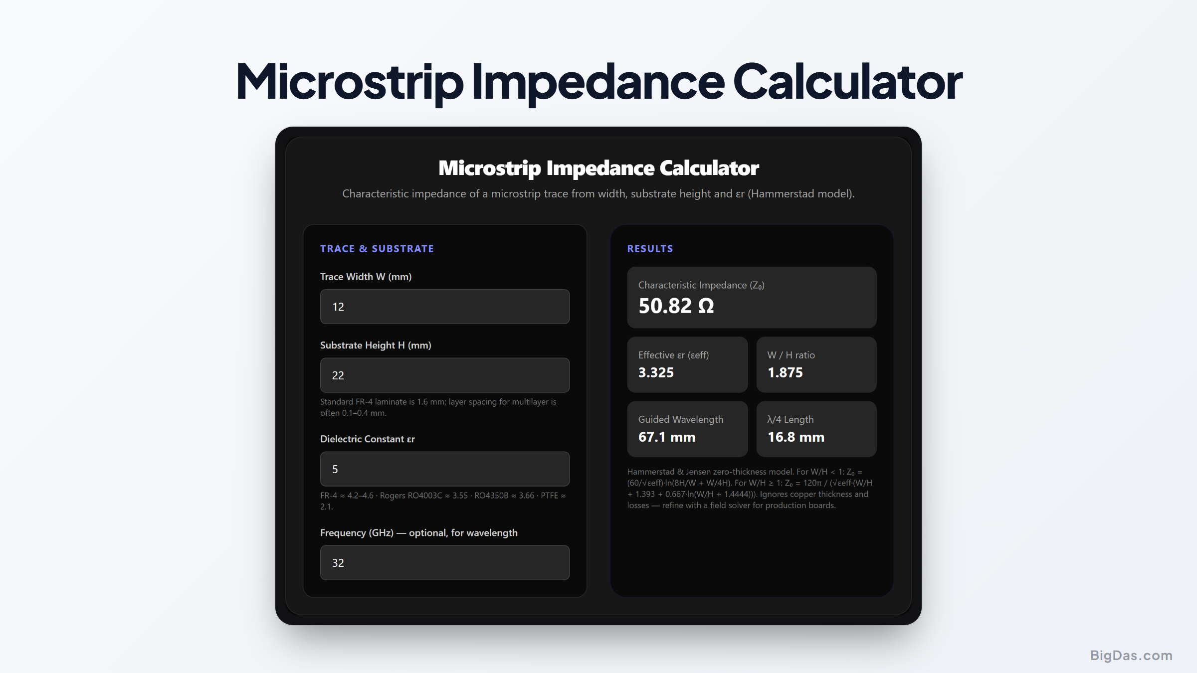
Microstrip Impedance Calculator
 Generated infographic and interface snapshot for Microstrip Impedance Calculator
Hit 50 Ω on your PCB the first time, classic Hammerstad microstrip math, live.
Free Microstrip Impedance Calculator Online. Big Das
Every RF trace and every controlled-impedance digital bus starts with the same question: how wide should this track be? Route it wrong and you get reflections, return-loss failures and flaky high-speed links. The Big Das Microstrip Impedance Calculator applies the industry-standard Hammerstad & Jensen equations to compute characteristic impedance from trace width, substrate height and dielectric constant, plus effective permittivity, guided wavelength and quarter-wave length for matching stubs.
What Is a Microstrip?
A microstrip is a copper trace on the surface of a PCB running above an internal ground plane, with air above and laminate below. Because the electromagnetic field lives partly in the dielectric and partly in air, it uses an effective permittivity (εeff) lower than the laminate's εr. That field split is what makes microstrip impedance depend on geometry, not just trace width alone.
How to Use the Calculator
- Enter the trace width W and substrate height H: same units (mm by default); H is the distance from the trace to its reference plane, not the total board thickness.
- Enter the dielectric constant εr of your laminate. FR-4 is roughly 4.2 to 4.6 at RF, Rogers materials are printed on the datasheet.
- Optionally add an operating frequency to get guided wavelength and λ/4 lengths for stubs and matching networks.
- Read Z₀, εeff and the W/H ratio live as you type, then iterate width until you hit your target (usually 50 Ω or 75 Ω).
The Formulas
The classic zero-thickness Hammerstad model:
- Effective permittivity:
εeff = (εr + 1)/2 + ((εr − 1)/2) / √(1 + 12H/W) - Narrow traces (W/H < 1):
Z₀ = (60/√εeff) × ln(8H/W + W/(4H)) - Wide traces (W/H ≥ 1):
Z₀ = 120π / (√εeff × (W/H + 1.393 + 0.667 × ln(W/H + 1.4444))) - Guided wavelength:
λg = c / (f × √εeff)
Accuracy is typically within 1 to 2% of a full field solver for 0.05 < W/H < 20.
Worked Examples
- 50 Ω on 1.6 mm FR-4 (εr 4.4): a 3.0 mm trace gives W/H ≈ 1.88 and Z₀ ≈ 50.5 Ω, the familiar "about double the laminate thickness" rule of thumb.
- 75 Ω video trace on the same stack: narrowing to ~1.2 mm lifts Z₀ to roughly 75 Ω.
- Quarter-wave stub at 2.45 GHz on FR-4: εeff ≈ 3.3, so λ/4 ≈ (122.4 / √3.3) / 4 ≈ 16.8 mm.
Common Use Cases
- Routing 50 Ω antenna feed lines for Wi-Fi, BLE, LoRa, GPS and cellular modules.
- Designing controlled-impedance high-speed digital runs (USB, HDMI, DDR) on standard FR-4.
- Sizing distributed filters, coupled lines, branches and λ/4 matching transformers.
- Sanity-checking a fab house's impedance stackup numbers before you commit a layout.
Frequently Asked Questions
Why doesn't this calculator include copper thickness?
The classic Hammerstad equations assume an infinitely thin trace. Real copper (18 to 70 µm) widens the effective conductor slightly and lowers Z₀ by 1 to 4% on thin laminates. For most FR-4 hobby and prototype work the zero-thickness model is within tolerance; use a 2D field solver for production boards.
The fab house quoted a different impedance for my geometry, who is right?
Possibly both: fabricators often use solver-based models with their exact stackup, dielectric tolerance and soldermask effects. A thin soldermask coating over a microstrip lowers impedance by a few ohms. Treat this calculator as the design starting point and the fab's stackup report as the final word.
What is the difference between microstrip and stripline?
Microstrip has air above the trace and dielectric below, so fields see two media (hence εeff). Stripline is buried between two planes, entirely inside the dielectric, its permittivity is simply εr and it needs wider traces for the same impedance. This calculator covers microstrip only.
Why does Z₀ fall when I widen the trace?
Widening W increases conductor-to-plane capacitance more than it decreases inductance, and Z₀ = √(L/C). The logarithmic formulas show this: Z₀ scales roughly with ln(H/W), so getting from 50 Ω to 75 Ω means shrinking the trace substantially.
How accurate is the wavelength output at GHz frequencies?
The quasi-TEM εeff model holds well into the low GHz range. Above roughly 10 GHz, dispersive effects and higher-order modes make εeff frequency-dependent, so verify with a full-wave solver for mmWave work.