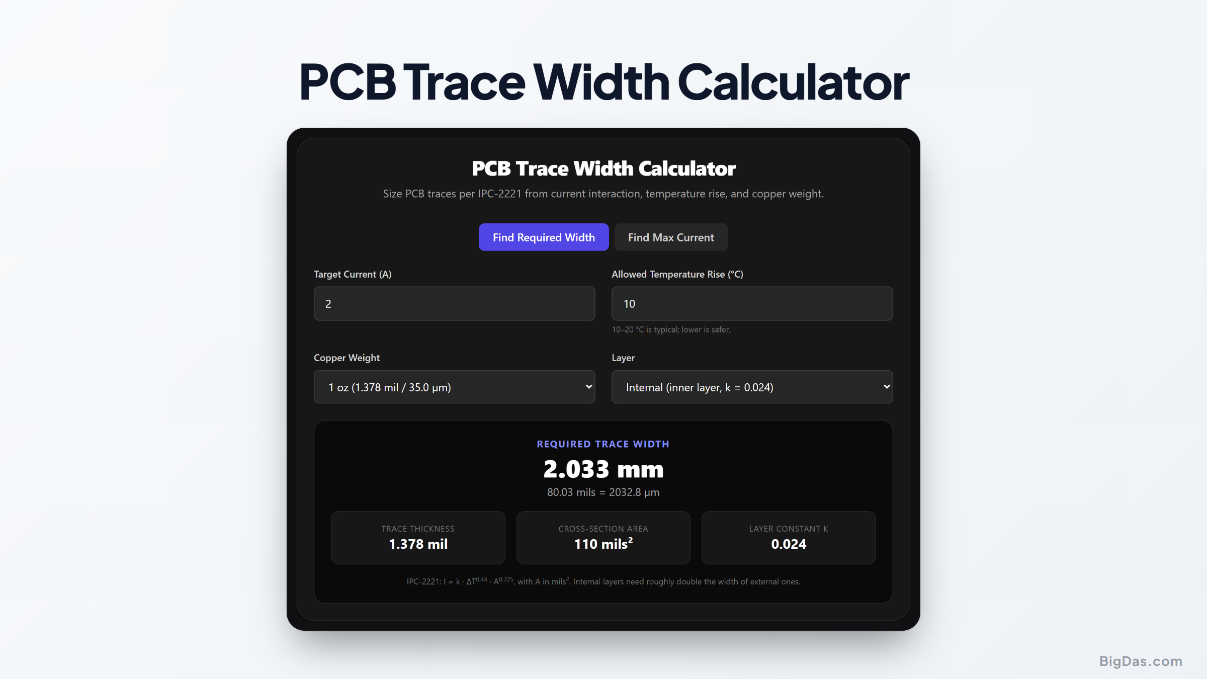
PCB Trace Width Calculator
 Generated infographic and interface snapshot for PCB Trace Width Calculator
Right-size your copper traces for current, heat, and layer placement.
Free PCB Trace Width Calculator Online. Big Das
Sending 2 A down a trace designed for a signal is the fastest way to turn a PCB into a fuse. The Big Das PCB Trace Width Calculator applies the IPC-2221 formula to give you the minimum trace width for your current and temperature budget, or, working in reverse, the maximum current a given trace can safely carry. Results update live in mm, mils, and µm, entirely in your browser.
What Is the IPC-2221 Trace Width Formula?
IPC-2221 is the standard for generic printed-board design. Its current-carrying equation relates current, allowed temperature rise, and the trace's cross-sectional area:
I = k × ΔT^0.44 × A^0.725
- I: current in amps
- k: 0.048 for external (outer) layers, 0.024 for internal layers
- ΔT: allowed temperature rise above ambient, in °C
- A: trace cross-sectional area in mils² (width × thickness)
Copper thickness comes from the board's copper weight: 1 oz = 1.378 mils (35 µm), 0.5 oz = 0.689 mil, 2 oz = 2.756 mils, and so on. Solving the equation for width gives the smallest trace that carries your current without exceeding the chosen temperature rise.
Why Internal Traces Need Double the Width
Outer-layer traces shed heat into the air; inner traces are sandwiched in FR-4, which insulates thermally. The standard halves the constant k to compensate, so an internal trace needs roughly twice the width for the same current and temperature rise.
How to Use the PCB Trace Width Calculator
- Pick the mode: "Find Required Width" or "Find Max Current".
- Enter the target current in amps: use your worst-case continuous current, not the average.
- Enter the allowed temperature rise: 10 °C is a common, conservative choice; 20 to 30 °C is acceptable when space is tight.
- Select the copper weight: 1 oz is the standard default; power boards often use 2 oz or more.
- Choose the layer: external for top/bottom copper, internal for inner layers.
- Read the results: required width in mm, mils, and µm (or max current, with headroom versus your target), plus the trace thickness and cross-section area.
The Formula, Solved Both Ways
Required width from current:
- A = (I ÷ (k × ΔT^0.44))^(1 ÷ 0.725), area in mils²
- Width = A ÷ thickness, where thickness (mils) = oz × 1.378
Max current from width:
- A = width (mils) × thickness (mils)
- I = k × ΔT^0.44 × A^0.725
The calculator also flags whether your existing trace passes or fails the current target, with the exact headroom or shortfall in amps.
Worked Examples
Example 1. Microcontroller power rail. Carry 2 A on an external 1 oz layer with a 10 °C rise:
- k = 0.048, A = (2 ÷ (0.048 × 10^0.44))^(1/0.725) ≈ 79.7 mils²
- Width = 79.7 ÷ 1.378 ≈ 57.8 mils ≈ 1.47 mm
Example 2. Same trace, internal layer. Switching k to 0.024 doubles the required area, so the same 2 A needs about 116 mils ≈ 2.94 mm.
Example 3. Reverse check. You already routed a 50 mil (1.27 mm) trace on 1 oz external copper. Max current at 10 °C rise:
- A = 50 × 1.378 = 68.9 mils²
- I = 0.048 × 10^0.44 × 68.9^0.725 ≈ 1.8 A, fine for a 1.5 A rail, tight for 2 A.
Common Use Cases
- Power rails: Size VCC and ground traces before routing.
- Motor and LED drivers: Verify high-current paths survive stall currents.
- USB and charging boards: Check 5 V/3 A paths on 1 oz copper.
- Design reviews: Confirm an existing trace width against its actual load.
- Layer-stack planning: Decide whether a power net needs an external pour.
Frequently Asked Questions
Is IPC-2221 conservative?
Yes, its curves were derived from limited historical data. The newer IPC-2152 standard often permits narrower traces, especially on thick cores. Many designers use IPC-2221 as a safe upper bound and validate thermally when space is critical.
What temperature rise should I choose?
10 °C for reliability-focused or enclosed products, 20 °C for general use, and up to 30 °C where space is scarce and the board runs in open air. Higher rise means more copper stress and more heat delivered to nearby components.
Why do internal traces need to be wider?
They cannot convect heat into air, heat must conduct through the laminate to reach a surface. IPC-2221 models this by halving the constant k, which roughly doubles the required width for the same current.
What does copper weight actually mean?
Ounces of copper per square foot of laminate. 1 oz/ft² spreads to 1.378 mils (35 µm) thick. Doubling the weight halves the required width for a given current, often cheaper than widening traces.
Can I use this for high-frequency signals?
For current capacity, yes. But RF and fast digital traces are usually sized by controlled impedance, not ampacity, the impedance target typically forces a width far narrower than the current limit demands.
Does the calculator handle zero or negative inputs?
No valid trace can come from non-positive current, temperature rise, or width, the tool shows an inline error instead of a meaningless or NaN result until you enter physically sensible values.
Is my design data uploaded anywhere?
No. Every calculation runs in your browser; nothing about your board leaves your machine.